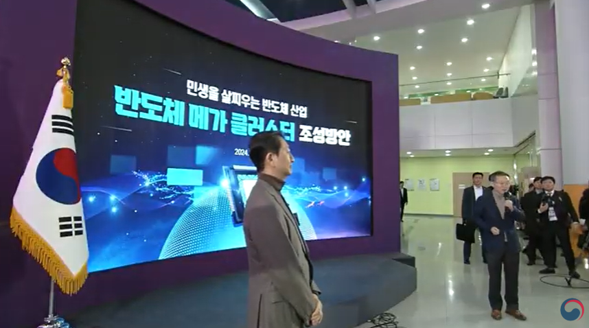
Government to Establish the World’s Largest and Most Advanced Mega Semiconductor Cluster

The government hosted the third policy debate with the public on January 15th, under the theme of “semiconductor industry benefitting people’s livelihoods.” In attendance were 110 citizens, including local residents, semiconductor industry representatives, students, and young researchers. The government presented the world’s largest and most advanced mega semiconductor cluster formation plan and engaged in discussions during the policy debate for the success of the new cluster.
The cluster encompasses areas with a number of semiconductor companies and related institutions in the southern part of Gyeonggi, including Pyeongtaek, Hwaseong, Yongin, Icheon, Anseong, Pangyo, and Suwon. Currently featuring 19 production fabs and 2 research fabs, the government plans to establish a total of 16 new fabs (13 production fabs, 3 research fabs) through the private sector’s investment of 622 trillion won by 2047, with 3 production fabs and 2 research fabs expected to be completed by 2027. Spanning 21.02 million square meters, the mega cluster is projected to produce 7.7 million wafers per month by 2030, making it the world’s largest. The government and businesses aim to create the world’s leading semiconductor production base by fostering an ecosystem within the cluster, including relevant material, component, and equipment companies, public semiconductor research institutes, fabless firms, and universities nurturing talent, producing cutting-edge memory, and establishing a 2nm or below process-based system semiconductor ecosystem.
The establishment of new fabs is anticipated to lead to direct economic effects and win-win growth in the ecosystem of material, component, equipment businesses and fabless firms, bringing production inducement effect of 650 trillion won.
As fab construction begins within the cluster, the production of equipment and raw materials by manufacturers is expected to result in approximately 1.93 million direct job creations. Additionally, an estimated 1.42 million indirect job creations are anticipated with the surrounding commercial areas revitalized and the expansion of infrastructure such as roads, electricity, and water facilities. When the 16 new fabs commence full operation, chip manufacturers are expected to employ over 70,000 experts. Furthermore, the revenue of supplier companies providing materials, components, and equipment for semiconductor fabs is projected to increase by approximately 204 trillion won, leading to the creation of around 40,000 jobs.
To sum up, it is anticipated that the 622 trillion won fab investment within the cluster will generate a total of 3.46 million direct and indirect jobs, contributing significantly to improvement of livelihoods. The government aims to accelerate the construction of the cluster, directly linked to economic growth and job creation, and plans to achieve semiconductor exports of 120 billion dollars and private sector’s investment exceeding 60 trillion won this year.
Minister of Science and ICT, Lee Jong Ho, emphasized that “Semiconductors are the cornerstone technology applied in AI and digital sector, telecommunications, quantum, bio, and are crucial to our economy.” He expressed his commitment to attentively listen to on-site voices to ensure the successful establishment of the mega cluster by securing cutting-edge technology and skilled professionals to position the country at the forefront of global semiconductor competition.
For further information, please contact the Public Relations Division of the Ministry of Science and ICT.
Editor Miso


